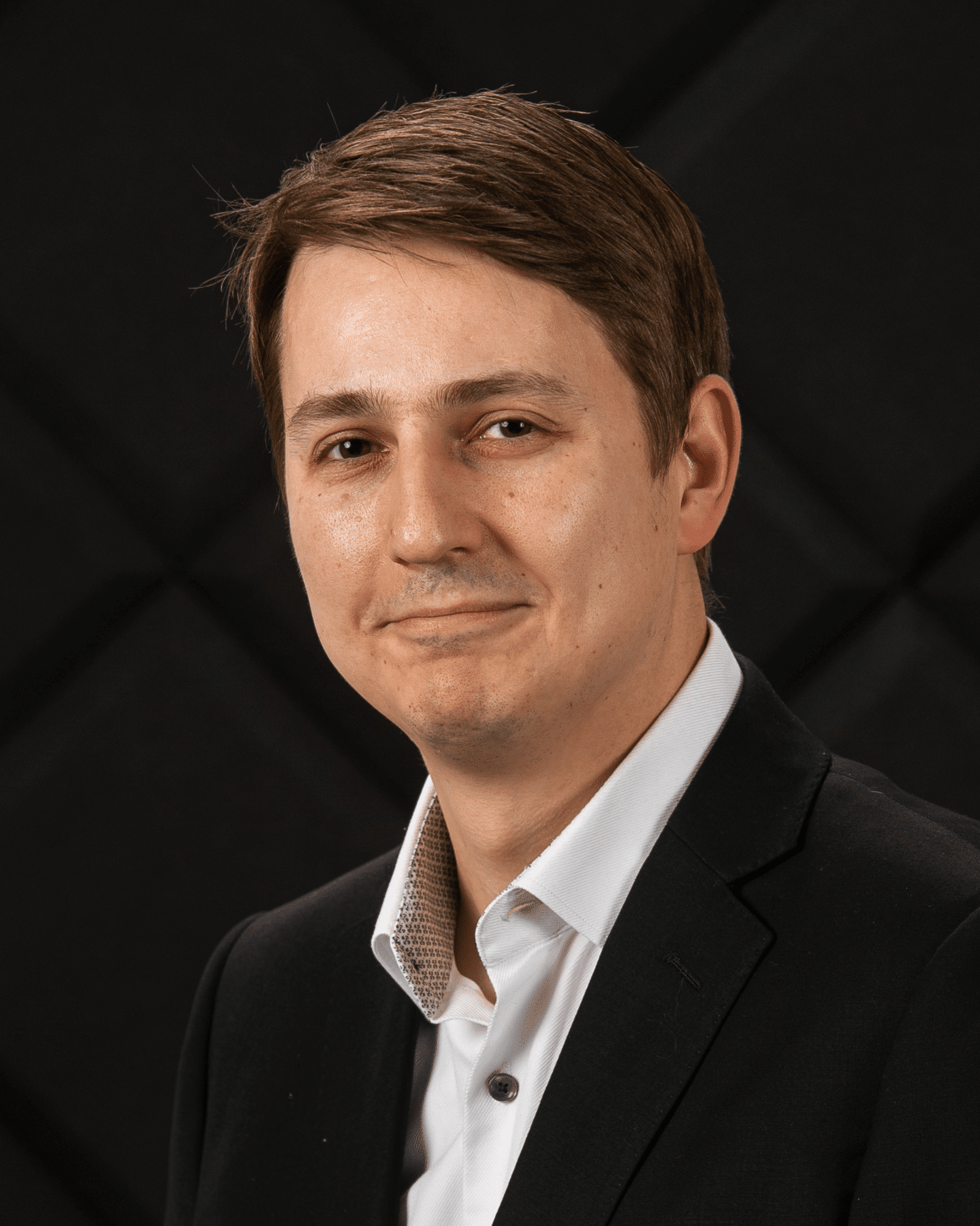
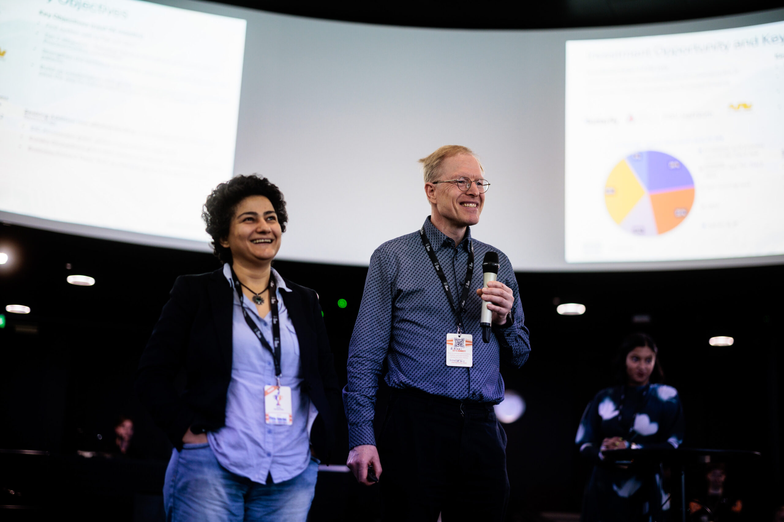
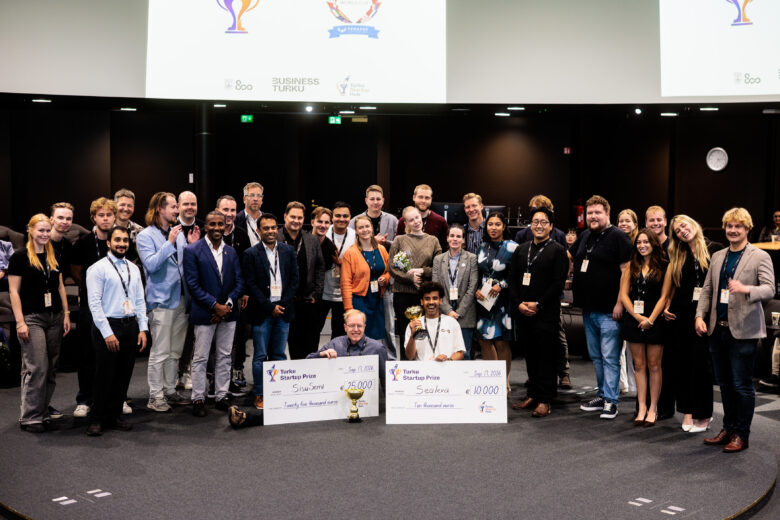
Turku-based SisuSemi won the main prize at the first-ever Turku Startup Prize competition on 16–17 September 2026. The company’s dream of taking atomically clean semiconductor technology to the global market is now one step closer.
Turku-based deep tech company SisuSemi is preparing for the Startup World Cup finals, which will be held in San Francisco in November.
The company secured its place in the finals by winning the Turku Startup Prize competition, organized by Turku Startup Hub. However, according to CEO Erkki Seppäläinen, the excitement soon gave way to practical preparations.
– We are now working hard to figure out how to make the most of this great opportunity. In addition to the prize money, this is a very significant victory for us.
SisuSemi develops a semiconductor surface-cleaning technology that removes contaminants from silicon wafers at the atomic level before new material layers are added. The technology enables the semiconductor industry to manufacture higher-quality products that consume less energy and have a longer lifespan.
The Startup World Cup pitch competition in San Francisco’s Silicon Valley offers an opportunity to make contacts with international investors and companies in the semiconductor industry. According to Seppäläinen, potential end customers include Intel, AMD and Texas Instruments because they all have their own chip manufacturing operations.
These companies manufacture processors for computers and servers, among other products, which are exactly the kinds of products that can benefit from SisuSemi’s technology for improving the cleanliness of silicon wafer surfaces.
– And of course, it would be great to meet Nvidia. Its chips are manufactured by TSMC in Taiwan but Nvidia could put pressure on the manufacturer. Our product would be important to them, too, because their products are among the newest and most advanced, where defects at the atomic level are most critical, Seppäläinen says.
The AI boom is creating opportunities also for SisuSemi
Seppäläinen compares the growth of the semiconductor industry driven by artificial intelligence to a gold rush.
– Demand for memory chips and other semiconductors has grown sharply, and manufacturers are making record profits. Memory prices have doubled since last year.
The availability of components has become a bottleneck. This is also creating a need for companies like SisuSemi, which is developing technology to make semiconductor manufacturing more efficient. Over the past year, SisuSemi has taken a major step forward.
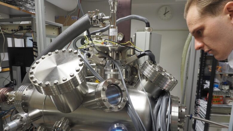
– A year ago, the AtomSeal device was still on the drawing board. In December, we installed it in our cleanroom, and we have since used it to produce samples for customer needs, working with silicon wafers up to 300 millimeters in diameter.
The AtomSeal device is an enclosed chamber that uses ultra-high vacuum technology to enable atomic-level purification. The 300-millimeter wafer size is widely used in industry, and represents more advanced technology that is only now being introduced in Finland.
One key development has been the use of lasers to heat silicon wafers.
– We are the first company in the world to have successfully used a laser to heat a 300-millimeter silicon wafer inside a vacuum chamber.
Removing the wrinkles – atomic-level purity matters
The technology developed by SisuSemi focuses on atomic-level purification (ALP), which is needed in semiconductor manufacturing. Finland has previously developed ALD technology (Atomic Layer Deposition), in which material is deposited onto the surface of a silicon wafer one atomic layer at a time.
– If the interface is not smooth and clean at the atomic level, it creates what are essentially wrinkles in every layer.
As semiconductor line widths are now around two nanometers, even the smallest irregularities on the surface can directly affect the electrical performance of the chips.
– It’s like having dirt on a window. When rain falls on the glass, the water behaves slightly differently where the dirt is. In the same way, impurities can prevent silicon wafers from functioning as intended.
And that can be very costly. According to Seppäläinen, manufacturers may have to discard as much as half of a production batch, representing up to two months of work.
The AtomSeal device developed by SisuSemi enables silicon wafer surfaces to be cleaned at the atomic level. The company’s goal is to develop an automated system for industrial use and build a business worth hundreds of millions of euros through equipment sales by 2035. Photo: Frans Rinne.
From research to commercial technology
The idea that the technology had commercial potential emerged in the late 2010s. The development of the technology into a business was made possible by Research to Business funding from Business Finland.
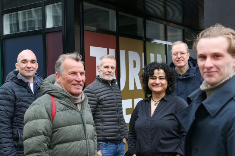
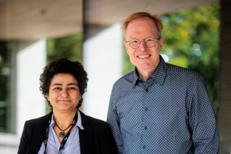
– Our CTO, Zahra ‘Elmira’ Jahanshah Rad, wrote her doctoral thesis on this subject and developed the prototype. Without the funding, none of this would have happened, Seppäläinen says.
Seppäläinen joined the company about three years ago. He is an industrial physicist and has worked, among other things, with optical fibre technology. He also has experience as a CEO and in board-level positions.
– I immediately recognised its significant international potential.
According to Erkki Seppäläinen, SisuSemi’s strength is based on more than 15 years of long-term research conducted at the University of Turku. Similar research has been carried out elsewhere in the world, but its commercialisation and scalability have not been considered realistic.
– SisuSemi has now found a solution to that problem!
The company is preparing for growth. In addition to the founding team, SisuSemi currently has three part-time employees, and plans to hire two more people. Following the funding round, the company intends to expand its sales team.
Networking is everything
SisuSemi aims to achieve annual revenue of hundreds of millions of euros by 2035. The company’s revenue would come from equipment sales. AtomSeal is currently still a partly manual prototype. Automating the process will speed up the handling of silicon wafers and turn the device into an industrial production system.
– Winning the competition in Turku gave SisuSemi valuable visibility. We need that visibility because we are seeking €3.5 million in funding.
Seppäläinen describes Turku’s startup community in positive terms. Although every company has its own deadlines and goals, he says that cooperation and support have been readily available.
– And of course, Business Turku has created an important framework for networking. The development of the startup ecosystem supports researchers and teams by bringing new perspectives to traditional research thinking. This has been evident in Turku for a long time, for example in biotechnology, Seppäläinen says.
According to Seppäläinen, many researchers need a push to commercialise their work. Encouraging examples and positive news can play an important role in this.
– Building a company that aims for international markets is a huge undertaking. Any help that makes the work of a startup entrepreneur easier is extremely valuable.
Text: Juha Riihimäki
Read more
Be part of our startup community!
Want to learn more about Turku Startup Hub? Whether you need help securing funding, growing your network, or finding the right space for your startup, we’re here to help. Explore the hub’s website or contact our experts today!